PID
Photo Imageable Dielectric
High‑performance photo‑imageable insulation material for forming micro‑circuit patterns in advanced semiconductor packages
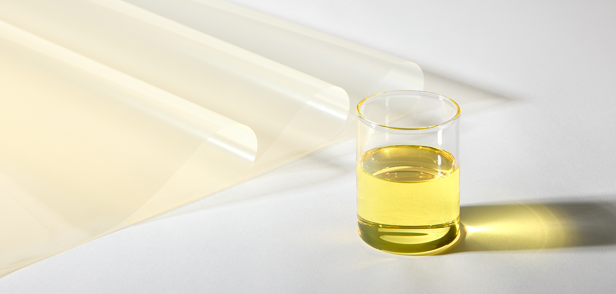
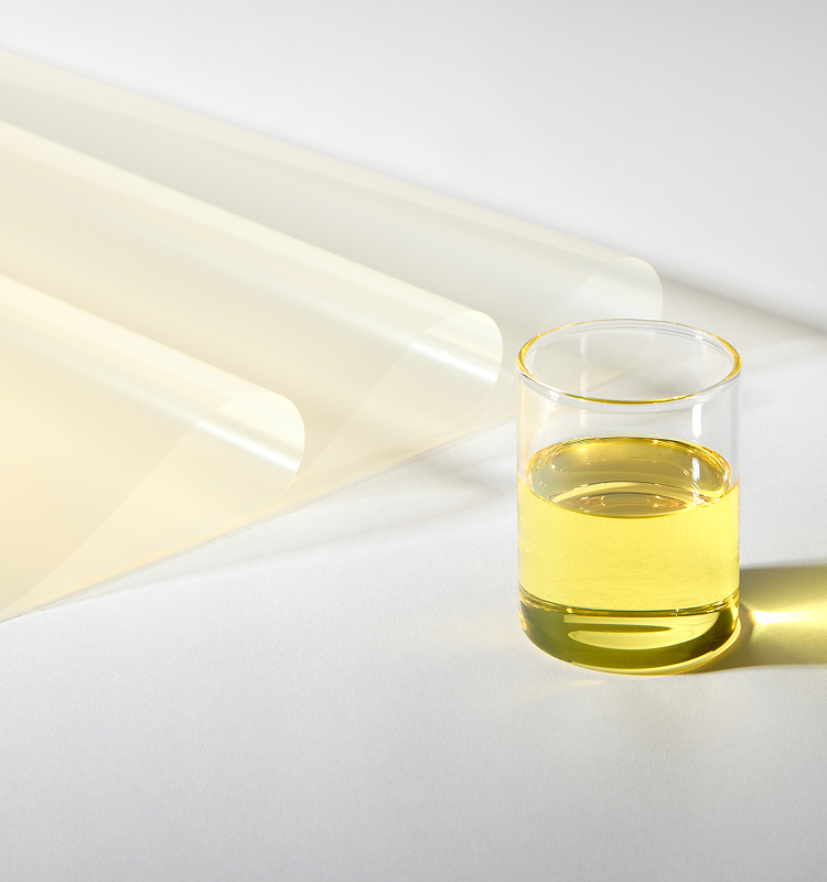
PID(Photo Imageable Dielectric) is a photosensitive insulating material used to form the fine circuit patterns that connect semiconductor chips to substrates in advanced semiconductor packages. It enhances package performance and reliability by enabling ultra‑fine circuit formation and ensuring stable electrical insulation.
As advances in AI increase the demand for higher‑performance semiconductors, LG Chem delivers PID materials featuring high‑resolution patterning and exceptional reliability essential for ultra‑fine circuit fabrication. Through an extensive lineup of liquid and film‑type products, we provide optimized material solutions tailored to customers’ process conditions and technical challenges.
Features
High Reliability
High‑resolution
Low‑temperature Curing
Eco‑friendly (PFAS Free)
Applications
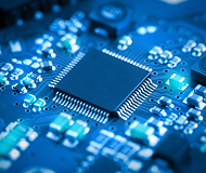
Power semiconductors
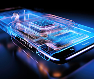
Mobile AP